

Computer Aids for VLSI Design
Steven M. Rubin
Copyright © 1994
|
Section 2 of 7 | |
The first type of synthesis tool to be discussed are those that work at a local level, within the cells of a chip. These tools generate the cell layout from a more abstract specification of the cell's functionality. To accomplish this task, the layout must typically be restricted to some regular pattern into which the original specification can be mapped. Thus PLA designs have rigid AND and OR planes of transistors, gate-arrays have fixed transistor pairs, and gate matrices have columns of gating material crossing rows of switchable interconnect.
All cell design has regularity; even layout produced by humans makes use of complex but regular patterns in the designer's mind that translate function to layout. These patterns guide the designer during layout and help to determine when the design is complete. Some artificial intelligence systems have attempted to codify these rules [Kim, McDermott and Siewiorek; Kowalski and Thomas; Kollaritsch and Weste; Mitchell, Steinberg and Schulman; Simoudis and Fickas], but the results often have noticeable patterns that are no better than the regular layout methods used by traditional generators. This simply shows that manual design is at the far end of a continuum of layout methods, used to build circuits from high-level functional specifications. The remainder of this section discusses a few of the regular styles of layout that are available today for cell synthesis.
This section was contributed by Sundaravarathan R. Iyengar, Case Western Reserve University.
Combinational circuit elements are an important part of any digital design. Three common methods of implementing a combinational block are random logic, read-only memory (ROM), and programmable logic array (PLA). In random-logic designs, the logic description of the circuit is directly translated into hardware structures such as AND and OR gates. The difficulty in this method is that the placement and interconnection cost is high. In a large system, this cost could be prohibitive. The ROM is useful for tabular data that has little regularity, but it is very wasteful of space for data that could be algorithmically derived. The PLA combines features of both other methods by allowing the designer to realize combinational design with programming taps on a logic array.
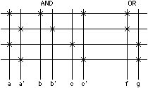
The PLA is made up of an AND plane and an OR plane. The AND plane produces product terms of input variables selected by the programming taps and the OR plane produces the sums of these product terms selected by a different set of programming taps. The symbolic representation of the places where the programming taps are placed is known as the personality matrix of the PLA. Figure 4.1 shows the generic structure of a PLA that programs these logic functions:
f = (a ![]() b
b ![]() (¬ c))
(¬ c)) ![]() ((¬ b)
((¬ b) ![]() (¬ a))
(¬ a))
g = (a ![]() c)
c) ![]() ((¬ a)
((¬ a) ![]() (¬ c))
(¬ c))
The PLA occupies less area on the silicon due to reduced interconnection wire space; however, it may be slower than purely random logic. A PLA can also be used as a compact finite state machine by feeding back part of its outputs to the inputs and clocking both sides. Normally, for high speed applications, the PLA is implemented as two NOR arrays. The inputs and outputs are inverted to preserve the AND-OR structure.
PLAs are popular because their generation can be automated, which frees the designer from spending valuable time creating random-logic gates. Since the PLA generator fixes the physical structure of the PLA, there arises the problem of accommodating the designer's special requirements, if any. The first requirement would be to reduce the area occupied by the PLA. Usually the personality matrix is so sparse that a straightforward mapping of the matrix to the silicon will result in wasted silicon area. Instead, the PLA is split and folded to reduce the area required for the physical implementation. Instead of having one AND plane and one OR plane, the PLA can be split into many more AND and OR planes. Also, the input and output columns can be moved and folded such that there are two to a column instead of the usual one. The rows can be similarly moved and folded. There have been many folding algorithms published [Hachtel, Newton, and Sangiovanni-Vincentelli].
The second important requirement is speed of operation. Switching speed is affected by parasitic capacitance and the driving capacities of input and pullup stages. Options to change the driving capacities of these stages would be a convenient addition to the PLA generator. This would involve estimating the parasitic capacitance and automatically sizing the driver transistors.
There are several more options that a programmer can provide for the user. For instance, there could be an option to correct electrical problems such as voltage buildups on the power and ground lines of the PLA. Sometimes, due to the interconnection requirements of the surrounding circuitry, it might be helpful to have the input and output entry points for the PLA appear on different sides of the layout. In a MOS PLA, for example, it is very simple to provide the outputs at the top of the PLA instead of at the bottom.
When a PLA is used as a finite-state machine, the input and output stages need to be clocked using two different phases or two different edges of the clock. Thus it is convenient to provide an option that generates clocked input and output stages when required. The clock, when off, would simply prevent the corresponding stages from loading. Regardless of clock usage, it is good to estimate the worst-case delay through the PLA (see Timing Verification, in Chapter 5). Since the timing of the clock phases is critical for proper operation of the PLA, this feature is important.
In conclusion, a PLA generator is a useful tool that forms an important part of many silicon compilers. Given a high-level algebraic or a truth-table description of the PLA, it generates the mask-level description, which can be fabricated directly. Since the generator uses a predetermined structure for the layout, it is important to be able modify it through high-level parameters. A parameterized generator is more useful than one that supports only a rigid structure. A simple way to implement the PLA generator with parameters is to first draw a sample PLA on a piece of paper (or on the screen) and to identify major building blocks. Typically there are input and output stages, pullups, programming taps, and the connection primitives that connect the planes together. Parameterizing each of these blocks allows more high-level options to be provided.
The gate-array is a popular technique used to design IC chips. Like the PLA, it contains a fixed mesh of unfinished layout that must be customized to yield the final circuit. Gate-arrays are more powerful, however, because the contents of the mesh is less structured so the interconnection options are more flexible. Gate-arrays exist in many forms with many names; for example, uncommitted logic arrays [Ramsay] and master-slice [Freeman and Freund].
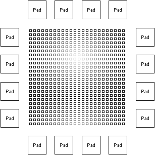
A typical gate-array is built from blocks that contain unconnected transistor pairs, although any simple component will do. An array of these blocks combined with I/O pads forms a complete integrated circuit and offers a wide range of digital electronic options (see Fig. 4.2). These blocks are internally customized by connecting the components to form various logical operators such as AND, OR, NOT, and so on. The blocks are also externally connected to produce the overall chip.
Designing a circuit using gate-arrays consists of specifying the internal and external connection requirements and then routing wires to produce the layout. There are high-level languages that help with the production of these connections. In these languages, designs can be easily specified by aggregating multiple blocks into larger functional units called macros. This is similar to macros in programming languages and it gives a semblance of hierarchy to the gate-array design. In addition to these macros, some gate-arrays have special-purpose circuitry, such as memory cells, so that these popular functions can be implemented more efficiently.
To aid in making connections, wire routing space is typically left between the gate-array blocks. Greater density is achieved in channel-less arrays, which leave no wiring space and then using an "etching" layer to eliminate circuitry and create space where it is needed. Another way to save the space between blocks is to have an extra layer of metal that is reserved exclusively for interconnect. This lets routing run across blocks rather than having to work around them. However, these connections can cross each other only in the area between blocks where it is possible to change layers.
Gate-array generation is another form of silicon compilation because a completed chip can be produced without any concern for the layout environment. Higher-level languages specify a circuit in terms of logic functions and the computer translates it into gate-array connections. Also, gate-arrays can be fabricated quickly because the blocks and pads are on a different layer than the interconnect. This results in many fewer fabrication masks to generate: Only one or two interconnect masks are needed for each new gate-array. These interconnect layers are also usually the last layers processed during fabrication, so they can be placed on top of nearly completed wafers that have been prepared in advance. Another advantage of gate-arrays is that they can take advantage of special manufacturing processes that produce high-speed parts.
The disadvantage of gate-arrays is that they are not optimal for any task. There are blocks that never get used and other blocks that are in short supply. Since block placement is done in advance, interconnect routing can become complex and the resulting long wires can slow down the circuit. Also, the design will not be compact since interblock spacing is fixed to allow worst-case routing needs. One estimate is that gate-arrays are three to six times less efficient than a custom layout [Heller].
The gate matrix (not to be confused with the gate-array) is the next step in the evolution of automatically generated layout from high-level specification [Lopez and Law]. Like the PLA, this layout has no fixed size; a gate matrix grows according to its complexity. Like all regular forms of layout, this one has its fixed aspects and its customizable aspects. In gate matrix layout the fixed design consists of vertical columns of polysilicon gating material. The customizable part is the metal and diffusion wires that run horizontally to interconnect and form gates with the columns.
It is a simple fact that layout is composed of transistors and the wires that connect these transistors. Weinberger observed that for MOS circuitry it is possible to transpose these transistors so that they reside on top of the connecting wires [Weinberger]. This is because the polysilicon wire in MOS is also the gate of a transistor. Converting a circuit to this form saves space and achieves regularity. The Weinberger array treats each column as a single NOR gate and requires all logic to be reduced to combinations of this element.
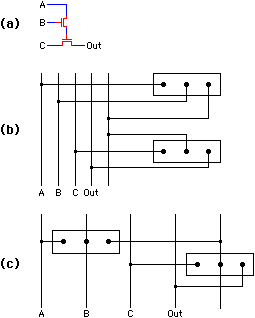
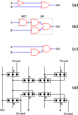
A gate matrix also makes the assumption that many of the vertical polysilicon lines are forming common circuit elements but the type of logic gate is unspecified (see Fig. 4.3). For example, each vertical line can be a NAND gate in nMOS by placing a load at the top of the line and ground on the bottom. Each gate on the column then acts as a pulldown that combines serially to form a multi-input NAND function. CMOS can also implement NAND gate matrices fairly easily [Weste and Eshraghian]. There are automatic systems to produce gate matrices from high-level circuit descriptions [Liu; Wing, Huang, and Wang]. Liu's system begins with logic gates, converts them to NANDs, reduces some of the redundant logic, and produces CMOS layout (see Fig. 4.4). The final step of assigning transistors to columns is prone to inefficiency since incorrect placement can result in long horizontal interconnect wires, and too many of these wires will cause the gate matrix to be slow and large.
Wing, Huang, and Wang have solved the transistor-placement problem in two steps. Each column is first ordered such that its transistors connect directly to both adjoining columns. This is essentially the greedy algorithm [Balraj and Foster]. A simple connectivity graph can be built and traversed for this task. There will certainly be gaps in the adjacency, but this initial placement is refined in the second step, which examines each transistor and computes the range of columns to which it is connected. This range is used to reorder the columns so that each transistor is closer to the center of its activity. The actual column and row spacing is then determined according to the interconnect needs. Rows are rearranged to obtain complete wiring and columns are widened if more space is needed.
Another automatic system for gate matrix optimization uses high-level rules to guide the process [Kollaritsch and Weste]. These rules examine the circuit, rearrange components, and compact. As with all rule-based systems, this one can be easily adjusted to provide better results in unusual cases.
In addition to gate matrices, there are many other ways to generate layout automatically from higher-level specifications. Diffusion line tracing is a method that strings together the transistors of a MOS design, connecting sources to drains as far as possible, and then routing the remaining polysilicon and metal connections [Nogatch and Hodges]. The storage/logic array [Goates, Harris, Oettel, and Waldron] is an enhanced PLA that contains memory elements so that state can be captured internally rather than having to loop around the outside of the array. The Tpack system allows designers to identify areas of a small layout that will be repeated according to a personality matrix [Mayo]. This allows large but regular circuits to be easily designed. Other methods are constantly being invented for the construction of layout. As these methods improve, they will approach the quality of hand layout and earn their place as the key component of silicon compilation.
The last synthesis tool to be discussed under the category of cell contents manipulation is compaction, which removes unnecessary space from a design by moving everything to its closest permissible distance. This step can be done on a completed chip but is usually done on a cell-by-cell basis to recover unused space as soon as possible.
The simplest compaction method, called one-dimensional compaction, works by squeezing space along the x axis and then along the y axis. This is repeated until no more space can be recovered [Williams; Hsueh and Pederson; Weste; Entenman and Daniel]. One-dimensional compaction is simple to do, runs fairly quickly, and will recover most of the savable space. More advanced techniques attempt to save additional space by jogging wires or moving components; thus they are performing placement, routing, and compaction all at once. These methods have combinatorial work to do and produce only slightly better results than simple compaction methods.
One-dimensional compaction uses information about components and their connecting wires. The wires that run perpendicular to the direction of compaction link a set of components into a single track that will adjust together. Components and tracks are typically represented with a graph that shows the movable objects and their movement limitations. For example, in Fig. 4.5 the track with components A, B, and C will move together when x-axis compaction is done, as will the track with components E, F, and G. Although a track may run for the entire length or width of the cell, it may also be treated as a locally connected piece of layout. This allows all unconnected parts of the design to compact properly, independent of other layout that may originate in the same row or column.
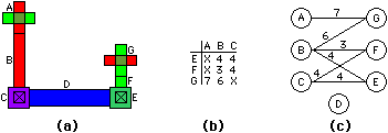
Compaction is done by adjusting the coordinates for each track. However, when virtual grid design styles are used, the initial spacings are all on a dimensionless grid, so the compaction process becomes one of assigning real coordinates to the tracks [Weste; Entenman and Daniel]. Regardless of the initial coordinate system, one-dimensional compaction must determine the minimum distance between two tracks of layout. This can be done by scanning all combinations of components in both tracks and computing the greatest design-rule spacing that is necessary. In Fig. 4.5, for example, transistors A and G must be 7 units apart from centerline to centerline, based on a 3-unit minimum diffusion spacing; 3 units between the centerline of A and its diffusion edge; and 1 unit between the centerline of G and its diffusion edge.
Each component must remain at a particular distance from its neighboring components, and this collection of distance constraints is found in the graph. Construction of the graph can be augmented by connectivity information so that electrically equivalent components are allowed to touch or overlap [Do and Dawson]. There can also be weighting factors in the graph to address nongeometric considerations such as the desire to keep diffusion lines short [Mosteller]. The graph, which has nodes for each component and arcs for each spacing rule, can be used to determine quickly the allowable separation of two tracks. Transistor A does not interact with objects E and F because they are not on the same level. Nevertheless, it is necessary to check for objects that are diagonally spaced because they may interact. Scanning the rest of these two columns shows that the 7-unit spacing is the worst case and thus defines the limit of compaction.
The previous example can also be used to illustrate the need for repeated application of one-dimensional compaction. The first x compaction places the two columns 7 units apart which is limited by the location of transistors A and G. It is possible, however, that during y compaction transistor G will move down but transistor A will not, due to other constraints. Then, the second pass of x compaction will bring the two columns to 6 units apart, defined by the minimum distance between wire B and transistor G. One-dimensional compaction is usually fast enough to be done continuously until there is no improvement made in either direction.
Although this method seems simple, there are pitfalls that must be observed. Weste observed that it is not sufficient to check only the next adjacent track when compacting. Pathological cases found in some environments cause layout two tracks away to present more severe constraints than does the layout in the immediately adjacent track [Weste]. Therefore the construction of the constraint graph must extend beyond the boundary formed by tracks of components, and must evaluate the worst-case spacing among all combinations of objects.
Another problem that can arise in alternating axes during one-dimensional compaction is that motion along one axis can block more significant motion along the other. With an interactive system, this can be controlled by having the designer specify areas and directions of compaction [Williams; Scott and Ousterhout; Mori]. Some systems allow designers to augment the spacing graph with their own constraints [Do and Dawson; Mosteller]. When these additional user constraints create an overconstrained situation, Do and Dawson leave the layout uncompacted with the hope that the orthogonal compaction phase will remove the blockage. Another feature that their interactive system provides is the notion of a fence that designers place to prevent unwanted mingling of components. Regardless of interaction flexibility, the problem remains that one-dimensional compaction has no global information to help it achieve the best results. What is needed is a way to relate the x and y constraints so that the sequencing of the process uses all of the available information.
Both x- and y-axis constraints can be incorporated into a single network to enable more global compaction [Watanabe]. This network has arcs between all components that may interact during compaction. These arcs are tagged to indicate whether they can act alone or can work in conjunction with a dual constraint that runs in a perpendicular direction. This notion of a dual constraint enables diagonally spaced components to compact in either direction. For example, two contacts that must remain 3 units apart can stay 3 units away in x, or 3 units away in y, but when they are placed on a diagonal it is not necessary to enforce both constraints. This is because diagonal constraints are spaced farther apart than is actually necessary.
Optimizing a two-axis constraint network involves a branch-and-bound technique that iteratively finds the longest path in either direction and removes one-half of a dual constraint to shorten that path. This can take much time on a large network, so it is useful to reduce the initial graph size as much as possible. Watanabe found a property of uncompacted layout that helps to reduce this network: If every component is viewed as a vertex and every wire as an edge, the initial design forms an uninterrupted area of polygons. A constraint between two components is not necessary if those components do not border on the same polygon.
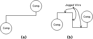
Humans often compact by jogging wires so that components can tuck into the tightest space. This can be done automatically by splitting wires at potential jog points so that the two halves can move independently. One observation is that good jog points occur where two parallel wires are connected by an orthogonal wire [Dunlop]. The orthogonal wire can be jogged to save space (see Fig. 4.6). Of course, jogs can be placed anywhere and the most general jog-insertion technique is to remove all wires and reroute them [Maley]. Routing methods will be discussed later in this chapter.
As a final consideration, it is possible to use simulated annealing as a model of compaction [Sechen and Sangiovanni-Vincentelli]. This technique, which is useful for many synthesis tasks, makes severe adjustments to the layout at the beginning and subsequently damps its action to make smaller changes, thus mimicking the annealing process of cooling molecules [Metropolis et al.]. By making component placement and orientation changes between compaction passes, each change can be seen either to help or to hurt the compaction. Major changes are tried first so that the overall layout configuration can be established. The minor changes are made last, in an attempt to save the small bits of space. This method consumes vast amounts of time but achieves very good results.
A more global issue in compaction is how to do it in a hierarchical environment. Typically, leaf cells are compacted first and then composition cells are adjusted to squeeze space around the leaf instances [Ackland and Weste]. This can cause problems when leaf-cell compaction realigns connection points, causing intercell connections to be broken. Although a hierarchical-layout constraint system, such as that in Electric (see Chapter 11), will keep these connections safe, most systems must do pitch matching (discussed later in the chapter) to ensure that hierarchical compaction will produce valid results [Weste; Entenman and Daniel].
Compaction is useful in improving productivity because it frees the designer from worries about proper spacing. With any compacter--even a simple one-dimensional compacter--layout can initially be done with coarse spacing so that the circuit can be better visualized. The designer is free to concentrate on the circuit and need not waste time scrutinizing the layout for unused space. Also, the existence of a compacter makes it easier to produce cell-contents generators because precise layout issues can be deferred. Finally, a compacter can be used to convert layout from one set of geometric design rules to another [Schiele].
|
Prev |  |
TOC | Next | |
 |