

Computer Aids for VLSI Design
Steven M. Rubin
Copyright © 1994
|
Section 2 of 5 | |
Before manufacturing a printed-circuit board, many designers build a prototype on a wire-wrap board. Wire-wrapping is the technique by which wires are attached to pins by being tightly wrapped around them. The electrical connection is good and yet changes are easily made.
Wire-wrap boards have a mesh of pins on one side connected to sockets on the other. IC packages are plugged into the sockets and interconnection is done on the pin side. Since the leads on ICs are typically 0.1 inch apart and since IC packages are often 0.3 inch wide or multiples thereof, the pins and sockets on a wire-wrap board are usually spaced 0.1 inch apart in columns spaced 0.3 inch apart. Additional pins and sockets are often found near the edge of the board to enable wiring of off-board connectors.
Since the wrapped wires are insulated, they can cross each other arbitrarily. Thus there is no routing problem, and the specific geometry of wire paths is not needed. All that matters is the location of the packages and the endpoints of connections. Essentially it is a netlist such as is given to switch-level simulators.
Although there are no rigid standards for this information, certain conventions should be followed. Wire-wrap boards typically identify their pins with alphabetic columns and numeric rows. The upper-left pin is A01 and the pin to its right is B01. Since the columns are spaced wider apart than are the rows, there are fewer columns and single letters often suffice to enumerate them. However, after column Z comes column AA, BB, and so on. To list the components on the board it is necessary to give the following information:
    Package name
    Package orientation
    Location of pin 1
For example, a line of text that reads 7404 1 M15 will place
a 74-04 chip in a vertical orientation (orientation number 1) with the first
pin of the chip at location M15 of the board.
As a double check, additional information may also be requested:
    Number of pins on the package
    Package width
    Location of the power pin
    Location of the ground pin
Wiring of the packages is then done by listing coordinate pairs to be
connected.
For example, the line C14 D25 will place a wire that runs from column C,
row 14 to column D, row 25.
Some wire-wrap formats allow definition of signal names so that symbolic pin locations can be given and color-coordinated wires can be used. Other options include the specification of twisted-pair wiring that requires two source and two destination pins.
Care should be taken when specifying the order of wires. Since wire-wrapping machines must make a physical movement when traveling from pin to pin, it is best to keep the start of one wire close to the end of the previous wire. This speeds wrapping time and saves money. It is tempting to use daisy chains, in which the next wire begins on the ending pin of the previous wire, since these are most efficient when specified in sequence. However, for ease of debugging, no wire should be covered by other wires that are further covered, because that will require too many removals to make a correction. The best order is to place every second wire in a run, and then to wrap the odd ones on top.
To generate the most useful wire-wrap boards, consider their purpose for existing. Wire-wrapping is a prototyping stage, which means that the designer will want to make changes to the circuit. Each change requires removal and rewrapping of wires. If the most volatile wires are wrapped last, they will be on top, which will make them easier to change. Power and ground wires rarely change so they should be specified first. Long wires should be placed later so they do not become trapped by short wires, which are more easily removed. User indication of volatility should even be allowed as a consideration when producing a wire-wrap specification.
A printed-circuit board is a sheet of nonconducting material, usually fiberglass, that has flat wires laid onto it. These wires run between holes in the board into which components will be attached. Most printed-circuit boards are multilayer boards that have wires on both sides and even on layers sandwiched inside the board.
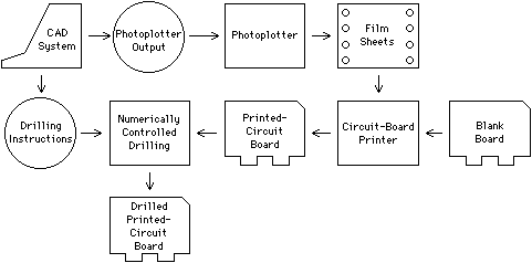
Each layer of a printed-circuit board is manufactured in a photographic process that uses a sheet of film to mask the location of wires. This film can be produced by hand or automatically from CAD system output. One popular automatic technique is the use of a photoplotter, which takes the output of a CAD system and produces film to be used in printed-circuit manufacturing (see Fig. 7.2).
The most popular format for photoplotter control is called Gerber format, created for Gerber Scientific Instrument Company machines [Gerber]. Today other companies' machines accept Gerber format, making this an industry standard.
Appendix A gives the details of Gerber format. Essentially, a Gerber file is a collection of ASCII commands and parameter values. The commands control a virtual pen that moves about the film drawing points, lines, curves, and text. Mode commands set state, and coordinate commands control the actual drawing. For example, once line-drawing mode is set, subsequent coordinate commands draw lines; when cubic-spline mode is set, subsequent coordinate commands are taken as inflection points for a curve. The virtual pen can be raised or lowered to switch between drawing and moving.
There is no hierarchy in Gerber format; the drawing commands are listed in the order to be performed. Thus an important consideration in producing these files is locality. Photoplotters take time to move the pen position, so the order of plotting should follow a minimal spatial path through the design to keep costs down. Some manufacturing companies even have programs to reorder plotting files so that the machine time is reduced. However, a good CAD system does things right the first time.
In addition to specifications for the wiring of a printed-circuit board, two other types of information should be available: the graphic (nonelectronic) artwork and the drilling instructions. Graphic artwork is an optional step that puts nonconducting ink on the printed-circuit board. This graphics contains helpful messages such as part numbers and connection names, which aid in the final production and debugging of the board. The methods for specifying and manufacturing this artwork are the same as for printed wiring: a Gerber file. Drilling instructions are necessary because they make the holes for the chip leads. These specifications are very different from wiring and artwork specifications, as the next section will illustrate.
As Fig. 7.2 shows, a printed-circuit board must not only be covered with wires, but also be drilled. The holes are used either for component connections or as through holes to connect different layers of the board. These holes are made by numerically controlled (NC) drilling machines, which take yet another format of file.
Numerically controlled drilling machines are very simple devices. They have a switchable drilling head that can automatically select from a set of tools, and they have a movable table that can place any part of the board under the head. Thus there are only two commands to an NC drilling machine:
Tdd
switches to tool dd, a number such as 01.
This tool switching takes time and so it should be done infrequently.
The second command makes the tool function by giving a coordinate in the form:
XdddddYddddd
where the ddddd values are five-digit coordinates, usually measured in inches, with an implied decimal point after the first two digits (dd.ddd). Since it is not known where the board will be placed on the drilling machine, the origin of the coordinate system should be adjustable so that any point on the board can be set to (0, 0) and the other coordinates will slide along. With NC drilling, as well as all formats, it is best to ask a manufacturing company to specify the precise style that it expects.
|
Prev |  |
TOC | Next | |
 |